AD652
Rev. C | Page 23 of 28
DELTA MODULATOR
The circuit of Figure 34 shows the AD652 configured as a delta
modulator. A reference voltage is applied to the input of the
integrator (Pin 7), which sets the steady state output frequency
at one-half of the AD652 full-scale frequency (1/4 of the clock
frequency). As a 0 V to 10 V input signal is applied to the
comparator (Pin 15), the output of the integrator attempts to
track this signal. For an input in an idling condition (dc), the
output frequency is one-half full scale. For positive-going
signals, the output frequency is between one-half full scale and
full scale; for negative-going signals, the output frequency is
between zero and one-half full scale. The output frequency
corresponds to the slope of the comparator input signal.
1
2
3
4
5
6
7
8
16
15
14
13
12
11
10
9
ONE
SHOT
AND
"D"
FLOP
Q CK
D
Q
1mA
20k&
AD652
SYNCHRONOUS
VOLTAGE-TO-
FREQUENCY
CONVERTER
5V
REFERENCE
+15V
360pF
0.0047?/SPAN>F
15V
CLOCK
V
IN
(0V TO 10V
F
OUT
+5V
0.01?/SPAN>F
1k&
Figure 34. Delta Modulator
Since the output frequency corresponds to the slope of the input
signal, the delta modulator acts as a differentiator. A delta
modulator is thus a direct way of finding the derivative of a
signal. This is useful in systems where, for example, a signal
corresponding to velocity exists, and it is desired to determine
acceleration.
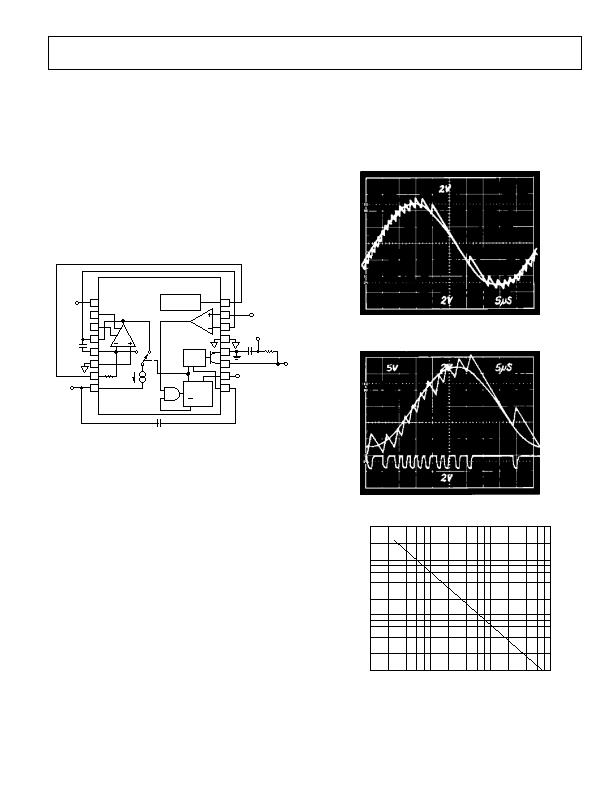
Figure 35 is a scope photo showing a 20 kHz, 0 V to 10 V sine
wave used as the input to the comparator and its ramp-wise
approximation at the integrator output. The clock frequency
used as 2 MHz and the integrating capacitor was 360 pF.
Figure 36 shows the same input signal and its ramp-wise
approximation, along with the output frequency corresponding
to the derivative of the input signal. In this case, the clock
frequency was 50 kHz.
The choice of an integrating capacitor is primarily dictated by
the input signal bandwidth. Figure 37 shows this relationship.
Note that as the value of CINT is lowered, the ramp size of the
integrator approximation becomes larger. This can be
compensated for by increasing the clock frequency. The effect of
the clock frequency on the ramp size is demonstrated in
Figure 35 and Figure 36.
Figure 35. Delta Modulator Input Signal and Ramp-Wise Approximation
Figure 36. Delta Modulator Input Signal Ramp-Wise Approximation and
Output Frequency
100
1k
10k
100
1k
10k
INPUT SIGNAL BANDWIDTH (Hz)
Figure 37. Maximum Integrating Cap Value vs. Input Signal Bandwidth
发布紧急采购,3分钟左右您将得到回复。
相关PDF资料
AD654JNZ/+
IC CONV VOLT-FREQ 500KHZ 8DIP
AD7740YRM
IC CONVERTER V TO FREQ 8-MSOP
ADM1070ARTZ-REEL7
IC CTRLR HOTSWAP -48V SOT23-6
ADM1073ARU-REEL
IC CTRLR HOTSWAP -48V 14TSSOP
ADM4210-2AUJZ-RL7
IC CTLR HOTSWAP LV TSOT23-6
ADVFC32SH
IC CONV V/F F/V MONO TO100-10
FAN4800ASNY
IC CTLR COMBO PFC/PWM 16-DIP
FAN4800AUN
IC PWM/PFC CTLR COMBO 16-MDIP
相关代理商/技术参数
AD652SQ/883B
功能描述:电压频率转换及频率电压转换 IC - SYNC V/F CONVERTER RoHS:否 制造商:Texas Instruments 全标度频率:4000 KHz 线性误差:+/- 1 % FSR 电源电压-最大: 电源电压-最小: 最大工作温度:+ 85 C 最小工作温度:- 25 C 安装风格:Through Hole 封装 / 箱体:PDIP-14 封装:Tube
AD652SQ/883B2
制造商:AD 制造商全称:Analog Devices 功能描述:Monolithic Synchronous Voltage-to-Frequency Converter
AD652SQ2
制造商:AD 制造商全称:Analog Devices 功能描述:Monolithic Synchronous Voltage-to-Frequency Converter
AD652SQ883B2
制造商:AD 制造商全称:Analog Devices 功能描述:Monolithic Synchronous Voltage-to-Frequency Converter
AD652SW
制造商:AD 制造商全称:Analog Devices 功能描述:Monolithic Synchronous Voltage-to-Frequency Converter
AD6532XBC
制造商:Analog Devices 功能描述:GSM/GPRS/EDGE DIGITAL BASEBAND PROCESSOR - Trays
AD6534BCP
制造商:Analog Devices 功能描述:
AD6534BCP-REEL
制造商:Analog Devices 功能描述: